EM and Thermal Analysis for RF Devices and System in HFSS Using 3D Component Package Model
Insights / whitepaper
Dec 19, 2024

Discover how cutting-edge electromagnetic (EM) and thermal simulation techniques in Ansys HFSS and Icepak streamline RF device development. This whitepaper explores a comprehensive approach to modeling RF power amplifier packages, addressing critical challenges like heat generation and system reliability.
Key Highlights:
Download the whitepaper now to see how advanced multi-physics simulation can transform your RF device design process, reducing development time and boosting product reliability.
Designing RF power amplifier packages that are reliable, efficient and cost-effective has always been a challenge for engineers. One of the main obstacles is performing mechanical thermal simulations on electromagnetic designs, which requires passing analysis results to thermal engineers and increasing development time. However, new techniques have been developed that allow designers to quickly gain thermal insight into their electromagnetic designs using HFSS.
RF GaN systems in package are known to generate a significant amount of heat during operation. This heat can have a detrimental effect on the system’s reliability and performance if not managed properly. Therefore, thermal management is essential for these systems. Accurate thermal simulation can help to optimize the system design and improve its efficiency. By modelling and analysing the heat distribution within the system, designers can identify potential hotspots and implement appropriate cooling measures. This will ensure that the system remains within safe operating temperatures, reducing the risk of component failure and prolonging the system’s lifespan.
Accurate thermal simulation is a critical aspect of optimizing the design and performance of various systems, including electronic devices. However, there are several challenges that need to be addressed to ensure accurate and reliable simulations. One of the significant challenges is obtaining accurate material properties, such as thermal conductivity and specific heat capacity. Another challenge is the multi-physics coupling that is often present in thermal simulations, where heat transfer is influenced by factors such as fluid flow and structural deformation. Additionally, complex geometries can make it difficult to accurately model the heat transfer and predict the temperature distribution. Finally, thermal simulations can be computationally intensive and require significant time and resources, making it essential to balance accuracy with practicality. Addressing these challenges is crucial to obtaining reliable and accurate thermal simulations that can help optimize system design and improve efficiency.
In this paper two case studies have been presented, showing the procedure of EM and thermal analysis in HFSS and Ice pack.
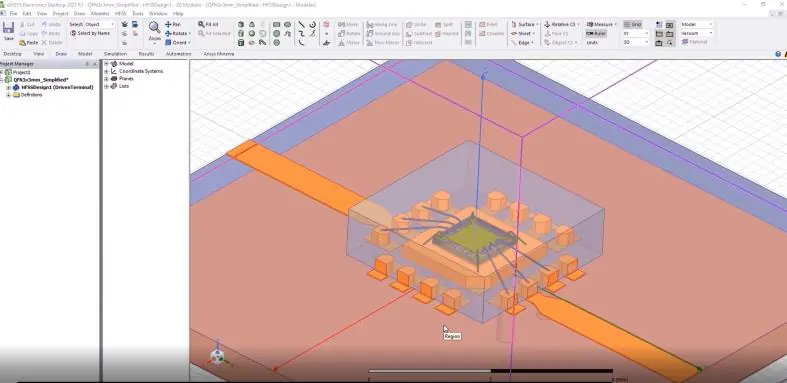
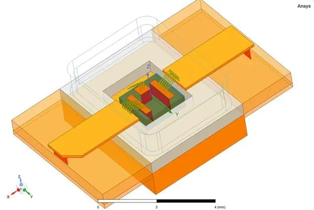
The first case study involved a GaN power amplifier in a package. HFSS was used to determine the 3D design of an RF power amplifier package that was mounted on a board with input and output transmission lines. The package had bond wires on the input, output, and ground plane, and the signal was transmitted from the input to the output. The thermal performance of this electromagnetic design was quickly obtained using the mechanical thermal solution in Ansys Electronics Desktop.
The 3D design which includes RF power amplifier with bond wires on the input, output, and ground plane has been modelled in HFSS shown in Figure 1.

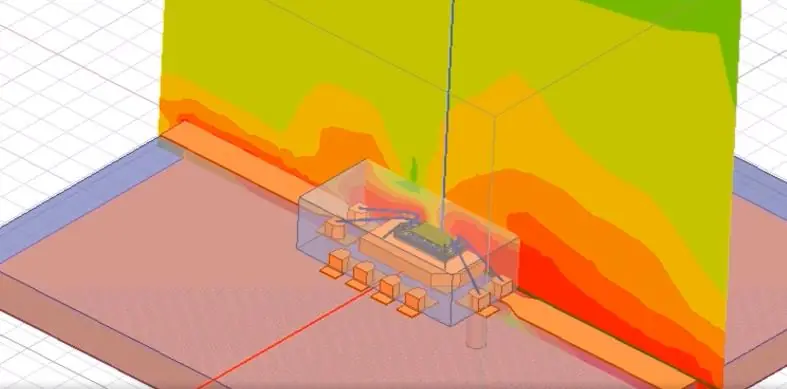
EM analysis in Figure 2 shows the electromagnetic field of the input signal is amplified and transferred to the output.
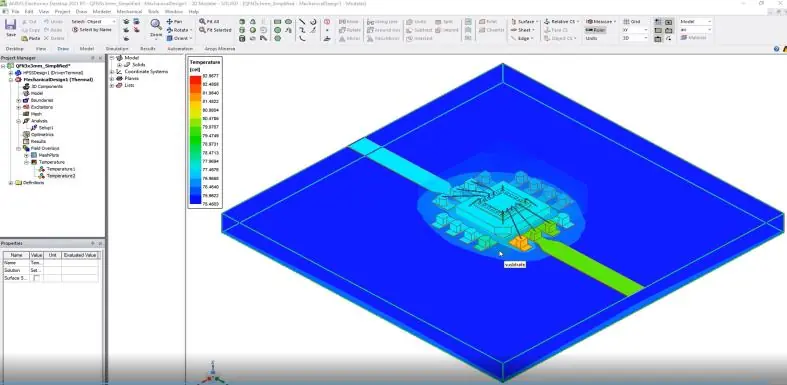
Next, the electromagnetic design from HFSS Maxwell was imported into the mechanical thermal solution in Electronics Desktop. The model was given life in the same GUI, and the model from the HFSS design was pasted. The Nickel design type was selected, and excitation loss was added to the model, linking it to the HFSS source project. This transferred the law of the dielectric and surface of the metal as heat loads for mechanical. Convection boundaries were also assigned to understand how the heat transferred from the surface of the package to the air surrounding it. Finally, thermal analysis was performed by importing the mesh generated from HFSS and running the simulation by clicking on the appropriate option. The temperature was plotted to obtain a complete temperature profile of the design shown in Figure 3.
Discrete power amplifier with packaged transistor
The Single Stage Amplifier Circuit Schematic is a widely used approach to amplify signals in electronic circuits. The first step in the workflow was to create the design of the package in HFSS. The package was an RF power amplifier with bond wires on the input, output, and ground plane, mounted on a board with input and output transmission lines. A circuit schematic of the amplifier was created, and the layout was generated using distributed elements.
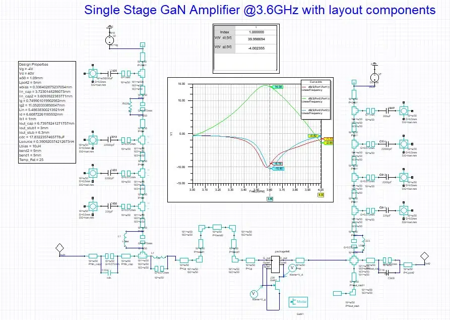
As given in Figure 4, a linear simulation of the amplifier in HFSS was performed to study its system-level performance. Co-simulation between the circuit and EM allowed the behaviour of the amplifier in the presence of electromagnetic fields to be understood. Next, the 3D Component feature in HFSS were used to further enhance the accuracy of the model. This enabled the effects of the package structure and geometry on the electromagnetic fields to be included.
After the EM analysis in HFSS was complete, the model was exported to the mechanical thermal solution in Electronics Desktop for thermal analysis. Convection boundaries were assigned to the model to understand how heat transferred from the surface of the package to the air surrounding it.
The mesh generated from HFSS was imported into Icepack for thermal analysis. A thermal simulation was performed to study the heat dissipation in the package. Appropriate thermal properties were assigned to the materials in the package and the surrounding environment, and the effects of conduction, convection, and radiation on the temperature distribution were considered.
After the simulation was complete, the results were analysed to determine the temperature profile of the package. This provided valuable thermal insights into the design, allowing the package to be optimized for better thermal performance.
To ensure optimal performance, it is crucial to match the amplifier components properly. In this design, the matching was performed using the Smith Tool and then translated into distributed and lumped element approaches, allowing for the inclusion of DC bias, AC coupling, and other necessary components. A package model, shown in Figure 5, was also included in the schematic for a complete layout, and bias networks were added to ensure wideband stability of the amplifier circuit. Incorporating these design elements into the Single Stage Amplifier Circuit Schematic allows for accurate simulations and optimizations, resulting in a highly efficient and optimized amplifier design.
To improve model fidelity, a 3D component model of a suitable package was constructed in HFSS using simplified dimensions taken from a Qorvo application note for a representative package model. This package model was used to perform accurate simulations and evaluate the package’s performance under different operating conditions, enabling package design optimization, which can significantly impact the overall device performance.
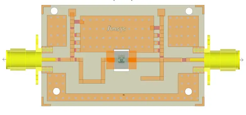
A large signal GaN HEMT was used as a representative test case, and a single-stage amplifier was designed with a circuit layout auto-generated from the circuit schematic using distributed elements. The layout was converted to an HFSS 3D layout EM model of the PCB layout, and 3D components were included, such as the HEMT package, coaxial adapters, bias pins, and metallic case. Co-simulation between Circuit and EM allowed for the study of the system-level performance of the amplifier, and a 3D component model of the package was added for additional model fidelity, enabling a thermal simulation of the package in Icepack.
To ensure accurate simulations, 3D components were used to add launchers and FET packages to the amplifier circuit design as shown in Figure 6. The 3D EM simulation in HFSS and thermal simulation in Icepack provided valuable insights into how electromagnetic waves and heat are distributed within the amplifier circuit design, allowing for the identification of areas that may be prone to overheating and the optimization of the design to ensure proper heat dissipation.
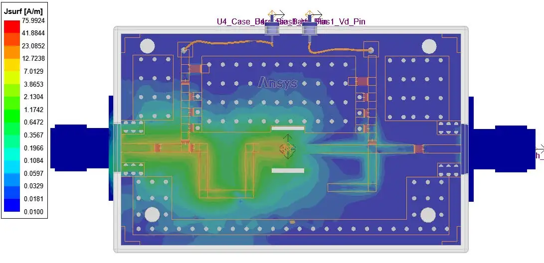
Figure 7 shows the current density at 3.6 GHz while using the push excitation from the circuit level. The result was obtained by the co-simulation between circuit and 3D EM analysis. The results from the thermal analysis in Ice pack is given in Figure 8.
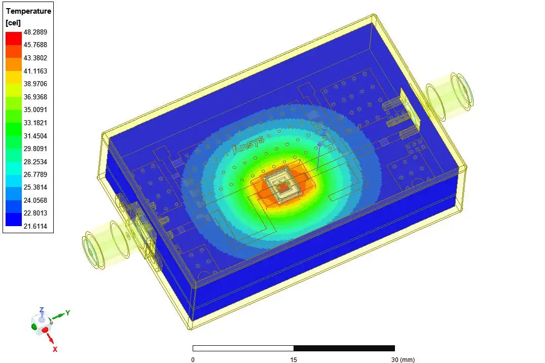
The integration of co-simulation between EM and Circuit models with thermal simulation in Icepack enables the design of PA models in packages with better performance and thermal management. This approach can be applied to other designs in the future, enabling design engineers to optimize their designs with ease and confidence. However, the result shown in Figure 8 is the thermal analysis of the design in Icepack which was not connected to the HFSS. This is an ongoing project which needs further work to generate the link between HFSS and Icepack.
The design of highly efficient and optimized amplifier circuits requires careful consideration of various factors, including matching of amplifier components, package design, and thermal management. The use of 3D component models and co-simulation between Circuit and EM models, as well as thermal simulation in tools such as Icepack, can significantly enhance the accuracy of simulations and enable engineers to optimize the design for better performance and thermal management.


We use cookies to enhance your browsing experience, personalize content and ads, analyze site traffic, and improve our services; by clicking "Accept," you consent to our use of cookies, and you can manage your preferences or learn more about our cookie policy on our Privacy Policy page.
