
Designing Below 3 GHz: Do You Really Need Full 3D EM Simulation?
If your product is not running at 28 GHz, 112 Gbps, or mmWave frequencies, it is easy to think full EM analysis is not relevant. That assumption is common, especially in teams working with more moderate interfaces such as USB 2.0, SPI, UART, MCU programming signals, and lower frequency RF or mixed signal designs.
But the real question is not whether your design is “high end enough” for simulation.
The real question is:
What level of simulation is actually needed for your design?
In many cases, designers working below 3 GHz can gain real value from simulation without jumping straight into full 3D EM analysis. At the same time, there are situations where 3D effects still matter, even at moderate frequencies.
This is where many electronics projects either over-engineer or under-analyze.
The good news is that you do not need extreme designs to benefit from simulation. You just need the right workflow.
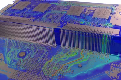
Modern electronics design has changed. Even below 3 GHz, products now include denser layouts, tighter spacing, faster edges, stricter EMC requirements, and more integration in a smaller space.
That means even “moderate” designs can suffer from:
In other words, lower frequency does not automatically mean low risk.
For many electronics engineering teams, the challenge is no longer whether to simulate. It is how to start without wasting time.
For many designs below 3 GHz, PCB level signal integrity and power integrity analysis is the right starting point.
This is especially true for designs using:
In these cases, tools such as Ansys SIwave often provide the right balance of speed, insight, and ease of use.
PCB level simulation is often enough when you want to evaluate:
For many electronics designers, this covers the majority of daily design questions.
Full 3D EM simulation is powerful, but it is not always the best first step. If you use a full 3D solver for every design, you may end up with:
That is why many successful teams start with a simpler PCB focused workflow first.
If your main questions are related to layout, PCB stackup, signal routing, charasteristic impedance, crosstalk, or power distribution, PCB level simulation is often enough.
This is especially true when working with moderate data rates and standard digital interfaces.
Even below 3 GHz, there are cases where full 3D EM simulation becomes important. This usually happens when the challenge is not only frequency, but geometry.
Examples include:
In these situations, the electromagnetic behavior cannot always be captured accurately with PCB level methods alone.
This is where Ansys HFSS becomes valuable.
HFSS is a full 3D EM solver designed for structures where field behavior, coupling, and geometry need to be captured in much more detail.
So the decision is not only about frequency. It is also about physical structure.
A simple way to think about it is this:
If the problem is mainly on the PCB, start with SIwave.
If the problem is driven by true 3D geometry, use HFSS.
For example:
A USB 2.0 route on a standard PCB may only need PCB level signal integrity checks.
But if that same product includes a connector transition, shield structure, cable interaction, or EMC hotspot near the enclosure, then full 3D EM analysis may be needed for that part of the design.
This is why the best approach is often not “all SIwave” or “all HFSS”.
It is a smart combination.
One of the biggest barriers in electronics simulation is the idea that you need to model everything at once.
You do not.
A much better approach is to start simple.
From a project perspective, this matters a lot.
If you use too little simulation, problems may appear late, during prototype testing or EMC certification.
If you use too much simulation too early, design work can slow down.
The goal is not to use the most advanced solver everywhere. The goal is to use the right level of simulation where it creates value.
For electronics teams working below 3 GHz, that often means:
That is the practical sweet spot.
At EDRMedeso, we help electronics designers choose the right simulation workflow for the actual design challenge.
That may mean helping your team:
For many teams, the hardest part is not using the software. It is knowing where to begin. That is exactly where we can help.
And in today’s electronics development environment, waiting too long to adopt simulation usually means more risk later in the project.
Designing below 3 GHz does not automatically mean you need full 3D EM simulation.
But it also does not mean simulation is unnecessary.
The key is simple:
Do not over engineer. Do not under analyze. Start with the right level of simulation.
If you are working on electronics design below 3 GHz and want to understand whether SIwave is enough or whether HFSS would add value, now is a good time to look at it.
EDRMedeso can help you assess your workflow, review your use case, and show you a practical path forward with Ansys simulation tools.
Get in touch with EDRMedeso to discuss your design, request a demo, or start a trial.
Request A Free Demo for Your PCB
