
Modern Electronics Design: How to Get Started
For many engineers, simulation still feels like something advanced, expensive, or only needed for very high-end projects.
In reality, simulation is an engineering tool. Just like an oscilloscope or a VNA, it gives you another way to understand your design.
It helps you answer questions such as:
Is my characteristic impedance under control?
Where is crosstalk coming from?
Will this via transition create a problem?
Is my PDN impedance acceptable?
Am I likely to run into EMC issues later?
These are not theoretical questions. They are the same issues engineers deal with every day in real products.
With electronics simulation, you can check them earlier, before the first prototype or before certification testing.
Do not start with software features. Start with a problem you already know. A good first simulation project could be:
This makes the learning process much easier. You are not trying to learn everything at once. You are using simulation to answer a design question that already matters to you.
If you are new to simulation, PCB level analysis is usually the best place to start. For many electronic design tasks, Ansys SIwave is a very practical starting point.
It is well suited for:
This is a good starting point because many of these tasks connect directly to real PCB design work.
You do not need to begin with the most advanced full 3D simulation.
Request your free demo for your PCB
One common concern is whether simulation will become too heavy or too slow. That usually happens when engineers jump too early into the most complex solver.
For long transmission lines, stackup related behavior, impedance control, crosstalk, power integrity, and many PCB level questions, SIwave is often enough. It gives fast results and supports quick design iteration.
That matters because early simulation should help you move faster, not slower.
At EDRMedeso, we help you determine the best tools for your requirements. We offer multiple options to assess this, for example, through free trials or Ansys Elastic Licensing.
Find out more about Ansys Elastic Licensing
This is one of the biggest benefits for engineers who are used to a test-driven workflow.
Higher data rates, DDR5 and beyond, high speed SerDes, tighter layouts, and stricter EMC requirements are no longer edge cases.
Traditional rules of thumb are breaking down. The classic 3W rule does not hold at 224 Gbps. Layout decisions that worked before can now lead to signal integrity issues, EMC failures, or unexpected coupling effects.
This is not something coming in the future. It is already here.
In the lab, you can measure what you built. In simulation, you can test what you have not built yet.
You can compare design options, adjust trace widths, study return paths, evaluate decoupling choices, and check the effect of layout changes before hardware is finalized. That gives much more insight during development. It also reduces the risk of late surprises.
A common concern from engineers new to simulation is simple:
Can I trust the results?
The answer is yes, but like lab work, good results depend on good setup and good engineering judgment.
Simulation can be correlated with measurements such as:
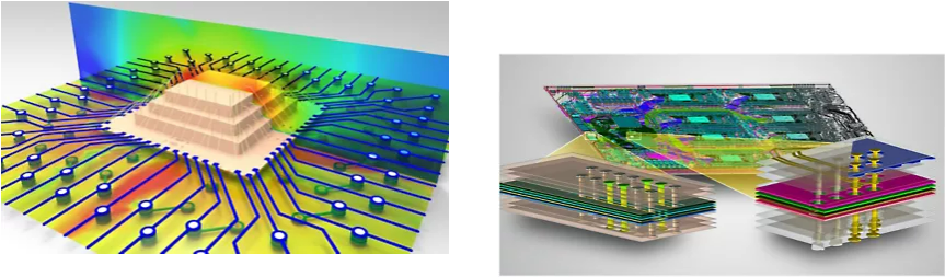
At the same time, simulation is especially valuable because it shows things you cannot easily see in the lab, such as field distribution and coupling paths.
That makes it a very useful complement to testing.
Do not try to simulate your whole product on day one.
Start with one layout.
One channel.
One PI problem.
One EMC concern.
Once you see how simulation helps explain real design behaviour, confidence grows quickly.
That is usually the turning point.
For many engineers, the first real value comes from small studies such as impedance, crosstalk, S-parameters, or DC IR drop. After that, it becomes much easier to expand into more advanced workflows.
This is where many teams save time.
You do not need to figure out the right simulation workflow alone.
At EDRMedeso, we help engineers get started. The goal is not to over-complicate the process. The goal is to help you choose the right level of simulation for your design.
That may mean starting with SIwave for PCB level analysis, then adding HFSS for critical 3D structures, and later building a workflow that connects simulation with your lab measurements and design process.
For teams working in electronics engineering, electrification, EMC, Signal Integrity, and Power Integrity, this can make a major difference in development speed and design confidence.
That said, not every design requires advanced simulation.
If you are working with low speed, simple circuits, traditional approaches may still be enough. But once you move into higher speed interfaces, dense PCBs, or EMC sensitive products, simulation becomes essential.
If you have strong hardware experience but have not yet adopted simulation in your workflow, this is the right place to start.
If you want a simple path to begin using simulation in modern electronics design, this is a good approach:
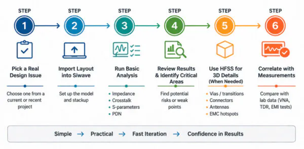
Step 1
Pick one real design issue from a current or recent project.
Step 2
Import the layout into SIwave and set up a basic analysis.
Step 3
Check impedance, crosstalk, S-parameters, or PDN behavior.
Step 4
Review the results and identify any critical structures.
Step 5
Use HFSS only for the areas that need full 3D electromagnetic detail.
Step 6
Compare the findings with your normal measurement workflow.
Moving from a test-driven approach to a simulation– driven design flow is not a matter of if. It is a matter of when.
If you have not started yet, the best first step is a simple one: choose a real problem and simulate it.
If you want to see how simulation could fit into your own electronic design workflow, we can help you to:
Request your free demo for your PCB
Webinar on Demand: Building a Connected Simulation Workflow for Power Signal and EMC Integrity
