
SIwave vs HFSS: How to Choose the Right Electronics Simulation Tool
One common question often comes up:
Should I use SIwave or HFSS?
Am I over-modelling? Or missing something critical?
SIwave vs HFSS: How to Choose the Right Electronics Simulation Tool, is our practical guide to help you decide.
In electronics simulation, there are two common pitfalls:
Using a full 3D solver for every scenario leads to:
Using simplified methods where full electromagnetic effects matter, can cause:
The goal is not to use the most advanced tool. The goal is to use the right tool for the problem.
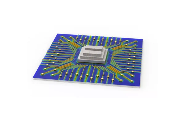
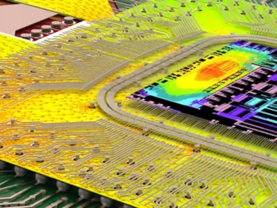
Ansys SIwave is designed for fast and efficient electronics design analysis at the PCB level.
It is the right choice when your focus is:
SIwave solves what is often called a 2.5D problem. This means it is optimized for planar PCB structures where most electromagnetic behavior follows predictable paths.
For many electronics engineering applications, especially below extreme data rates, SIwave provides all the accuracy you need with much faster turnaround time.
This is critical when you are iterating your design and testing multiple scenarios.
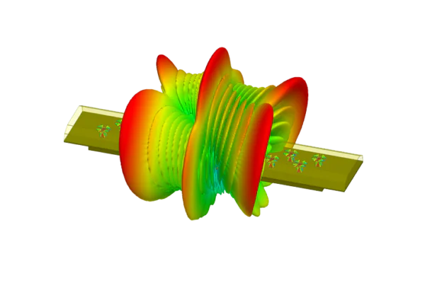
Ansys HFSS is a full 3D electromagnetic solver. It is built for problems where geometry and fields are truly three dimensional.
For example, back drilling effects, BGA breakouts, and connector transitions often require full 3D modeling to capture the real behavior.
At higher frequencies, wavelength becomes comparable to physical dimensions. This is where simplified assumptions start to break down, and 3D electronics simulation must capture full field interactions. HFSS provides that level of accuracy.

A common question is at what frequency the transition from SIwave to HFSS becomes mandatory. The honest answer? It depends on the design and accuracy requirements.
However, if a single frequency must be given, 10 GHz is a useful rule of thumb. Beyond this point, it is worth actively evaluating whether a 2.5D approach is still sufficient, or if a full 3D solver is needed.
This is not a strict boundary – some PCB structures can be modeled accurately with 2.5D methods even above 10 GHz, while complex geometries may require 3D analysis at lower frequencies. However, 10 GHz serves as a clear and memorable trigger to reassess your simulation approach.
Request a Free Demo for Your PCB
In practice, most advanced teams do not choose SIwave or HFSS. They use both.
A typical workflow in electronics design and electrification projects looks like this:
Optimize stackup, trace widths, and general layout
Analyze vias structures, connectors, and localized 3D structures in HFSS
Confirm performance before manufacturing or certification
This hybrid approach balances speed and accuracy and avoids unnecessary simulation time, while still capturing critical electromagnetic effects.
As designs move toward higher data rates, such as DDR5 or high-speed SerDes, traditional design rules become less reliable and the effects below start to play a larger role:
In these cases, moving from SIwave to HFSS is not a question of preference. It becomes a requirement.
If you are unsure which tool to use, start with these questions:
Start simple. Increase complexity only where needed.
SIwave and HFSS are not competing tools – they are complementary.
In electronics engineering, the goal is not to use the most powerful solver, but the most appropriate solution for the problem at hand. The right choice enables faster insight earlier in the design process, helping to avoid surprises in testing and reducing risk in production.
As designs grow more complex and frequencies increase, understanding when a 2.5D approach is sufficient and when full 3D analysis is required becomes an essential engineering skill.
