Integrating HF and Optics: How Ansys Makes It Possible
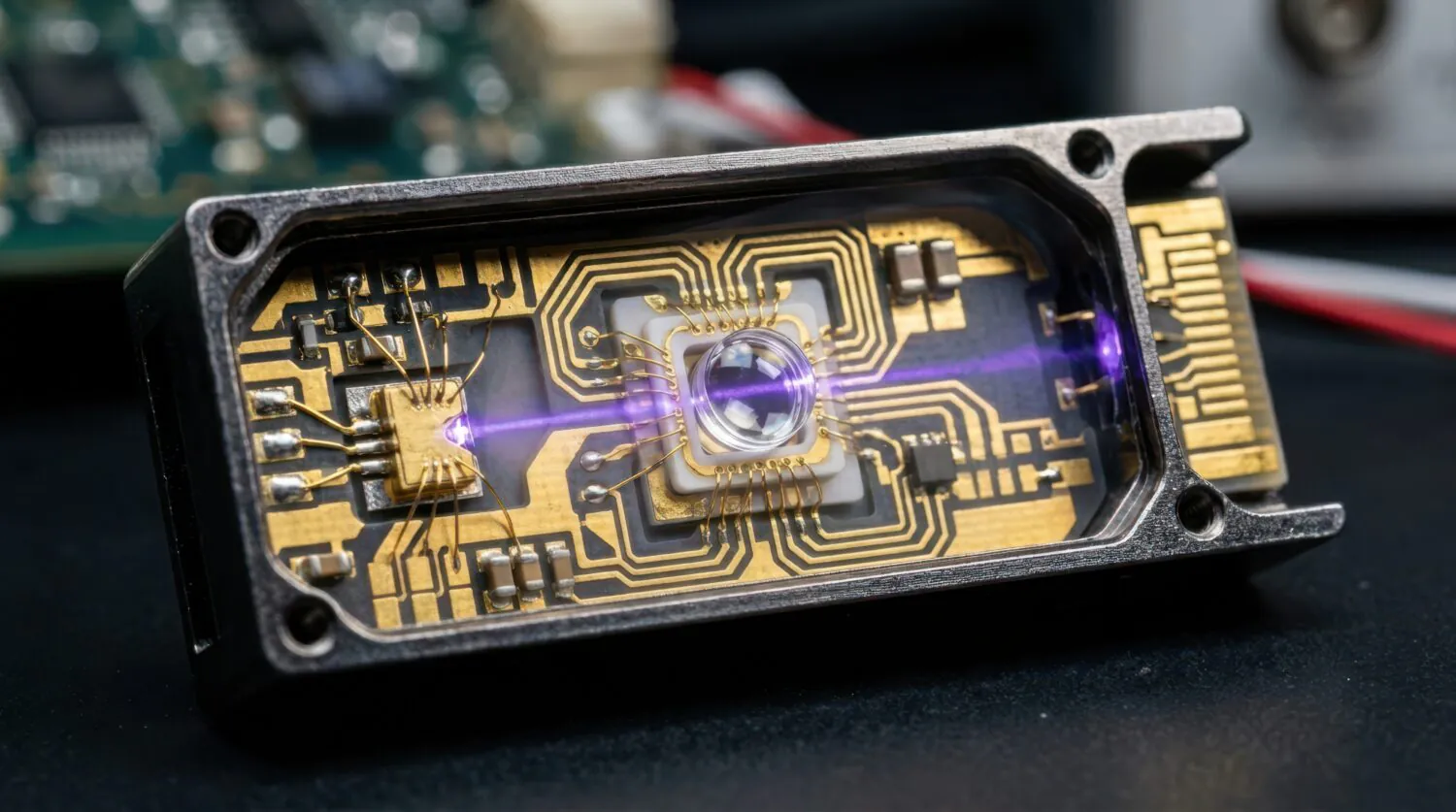

Integrating high frequency electronics and optics is becoming essential in modern engineering, where high frequency electronics and photonic systems must work seamlessly together.
As data rates increase, traditional electrical connections are reaching their limits.
Copper traces and electrical interconnects face challenges such as:
To overcome these limits, companies are moving toward optical communication inside electronic systems.
This includes:
In these systems, electrical signals are converted into optical signals, transmitted as light, and then converted back into electrical signals.
That means one thing: you now need to design electronics and optics together.
When electronics and optics are combined, the complexity increases quickly.
You are no longer dealing with only electrical behaviour. There is now a need to consider:
Traditional tools are not enough on their own. You need a way to simulate the full system. This makes electronics and optics integration critical for achieving accurate system-level performance.
Here is where Ansys stands out. Instead of treating electronics and optics separately, Ansys provides a connected simulation ecosystem.
Ansys HFSS is used to simulate high frequency electromagnetic behaviour such as:
HFSS allows engineers to accurately model high speed and RF systems, reducing the need for multiple physical prototypes and saving time and cost .
For optical design, Ansys provides:
These tools allow engineers to design and optimize optical systems from nano scale photonic structures to full optical systems.
The real power comes from integration.
With Ansys, electrical and optical simulations can be connected into a single workflow.
For example:
In one example, Ansys tools are used to simulate an optical transceiver where an electrical IC and a photonic IC are connected and analyzed together in a single workflow. This means engineers can understand how the entire system behaves, not just individual parts.
Modern systems operate across different scales:
Ansys tools allow engineers to connect these scales and simulate both wave optics and ray tracing in the same design flow. This is critical for designing real world products.
This integration is already being used in:
As bandwidth demands increase, these systems are becoming standard, not experimental.
For teams working with advanced electronics, this shift has real impact.
Without integrated simulation:
With integrated simulation:
In simple terms, you move from guessing how systems interact to actually understanding it.
One common misconception is that integrating electronics and optics requires a complete transformation.
It does not.
A practical approach is:
Step 1: Start with your current domain, electronics or optics.
Step 2: Identify where interaction happens, such as a transceiver or optical interface.
Step 3: Introduce simulation for that interface.
Step 4: Gradually connect electrical and optical workflows.
This step-by-step approach reduces complexity and delivers value quickly.
Understanding where to start is often the hardest part.
At EDRMedeso, we help companies:
Whether you are working with high-speed electronics, photonics, or system integration, the goal is the same:
Make better decisions earlier in the design process.
The integration of high frequency electronics and optics is not a niche topic anymore. It is becoming a standard requirement in modern product development. Companies that understand and simulate these interactions early will move faster and reduce risk. Those that do not will face increasing complexity later in the process.
By enabling electronics and optics integration, Ansys helps engineers design more reliable and efficient systems across industries.
Working with high-speed electronics, optical systems, or next generation communication technologies? Now is the time to explore integration and see how Ansys can support your design workflow.
Contact EDRMedeso to request a demo or discussion