The Invisible Process Behind Reliable Technology: A Typical EMC Workflow with Ansys Tools

Every modern product, from smartphones to factory robots, relies on tiny electronic systems that must work together. Each signal, each connector, and each component needs to perform in harmony. A small change in one part can affect the whole.
Modern electronic systems are pushing performance limits across every domain. The picture below illustrates how engineers can connect every stage of the design flow using Ansys simulation tools, creating a unified digital thread from EDA to electromagnetic and thermal verification.
The integration of SIwave, Q3D, HFSS, Circuit, and Icepak creates a continuous simulation thread across multiple domains. Engineers no longer need to manually transfer data or rebuild models between tools. Instead, they can work within a connected ecosystem that supports electrical, electromagnetic, and thermal analysis simultaneously.
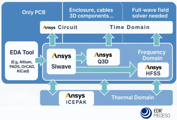
A Typical EMC Workflow with Ansys tools.
The process begins with an EDA tool such as Altium, PADS, OrCAD, or KiCad. This is where the printed circuit board is designed. Once that design is ready, the next question appears: how will it behave when electricity flows through it?
Ansys SIwave helps find the answer. It transforms the layout into a model that shows how signals travel across the board, how power is distributed, and where interference might appear. The results tell engineers what would happen if that design were built and tested in the lab.
Ansys SIwave is built for analyzing signal integrity (SI), power integrity (PI), and electromagnetic interference (EMI). It’s the link between layout and physics. Moreover, SIwave connects directly to Ansys Q3D Extractor for detailed RLC parasitic extraction, enabling engineers to create precise SPICE or S-parameter models for system-level simulation.
Webinar on Demand: Solving EMI/EMC Challenges in Electronics Design
Real products are rarely limited to a single circuit board. They include connectors, cables, and metal enclosures. These elements can change how electromagnetic waves behave.
That is where Ansys Q3D and HFSS come in. Q3D captures the electrical details of connections, while HFSS allows engineers to explore how fields move through three-dimensional structures. It helps answer questions such as: Will the antenna in a new phone communicate efficiently? Will a car’s radar stay accurate in a metal frame?
With these insights, design teams can see how the invisible electromagnetic world shapes real performance.
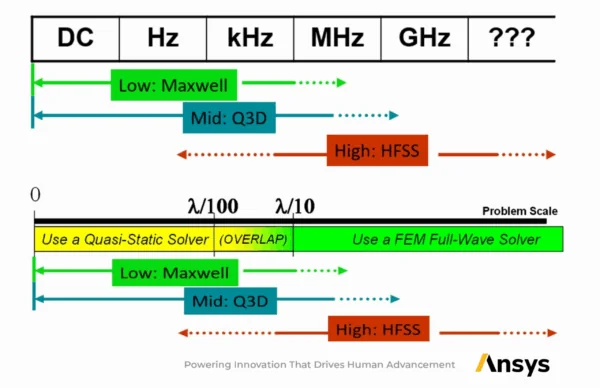
High versus Low Frequency Wavelenght Categorization.
HFSS delivers gold-standard accuracy for electromagnetic simulations in the frequency domain. It helps engineers visualize how 3D geometries impact system performance, identify resonances, and ensure compliance with EMC standards.
Therefore, when a project demands detailed 3D field analysis, HFSS complements SIwave and Q3D perfectly. By combining these tools, engineers can scale smoothly from board-level detail to complete 3D electromagnetic system analysis without losing data fidelity.
After frequency-domain analysis, engineers move to Ansys Circuit to study how signals behave over time. How does a system react when a processor starts or a motor switches on? This step connects earlier results to complete time-based performance checks.
This allows engineers to evaluate transient responses, switching behavior, and system-level interactions across mixed-signal designs, all using a single, interconnected workflow.
Electrical performance means little without thermal stability. Ansys Icepak helps engineers study how temperature spreads across a product, how airflow cools it, and how design choices affect reliability.
The results might answer questions such as: Will a smartphone stay within a safe temperature range while charging? Will a power converter in an industrial machine remain cool during continuous operation?
Ansys Icepak links directly with electrical simulation to study how temperature spreads inside a product. It helps determine if a design can handle power load, how air moves through a device, and where cooling is required. In practice, this means fewer unexpected shutdowns, longer component life, and stable performance under load.
All these tools together create one unified simulation environment. Engineers can move from idea to verified design without repeating work or losing data. The same process helps detect performance problems early and reduce the risk of interference or overheating.
This workflow is not limited to a single industry. It supports everything from consumer electronics to transportation, energy, and communication technology. The goal is the same in every case: to ensure that the product you use every day performs as intended.
The workflow allows:
The next time a new device works exactly as expected, you’ll know about the connected tools and the hidden process that made it all work. This is what we do best at EDRMedeso. Let us help you get started with world leading simulation tools and expert training.